In a field where atomic-scale control defines the future of electronics, Electron Beam Lithography (EBL) has emerged not just as a niche tool, but as a fundamental enabler — particularly for compound semiconductors, which are increasingly crucial to next-generation technologies like high-frequency communication, quantum computing, and optoelectronics.
EBL’s ability to draw arbitrary, ultra-fine patterns directly onto substrates without a physical mask makes it uniquely suited to handle the material, structural, and process-specific challenges of compound semiconductors such as GaAs, InP, GaN, and their alloys.
Let’s explore why this matters.
The Rise of Compound Semiconductors
For decades, silicon has dominated the semiconductor industry, but its limitations are becoming more pronounced as we push into terahertz communication, power electronics, and quantum devices. This is where compound semiconductors come in.
What makes them special?
- Direct bandgaps: Enabling efficient light emission — essential for LEDs, lasers, and photonic devices.
- High electron mobility: Supporting faster switching speeds in transistors.
- Wide bandgap properties (e.g., GaN): They are robust against high voltages, temperatures, and radiation.
These advantages open up applications that silicon simply can’t handle — but they come at a cost. Compound semiconductors are more expensive, chemically sensitive, and often mechanically fragile. Their heterostructures — layered combinations of different materials — require surgical precision in both growth and patterning.
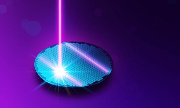
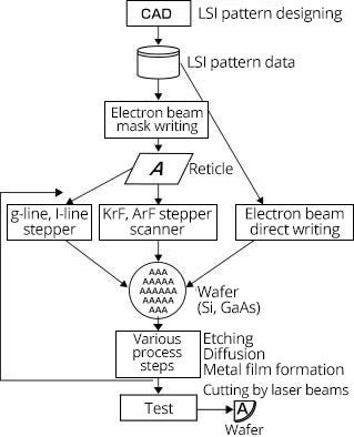
EBL: Writing Patterns with Electrons, Not Light
Electron Beam Lithography doesn’t rely on photomasks. Instead, a highly focused electron beam — with diameters as small as 1–5 nm — is rastered or vector-scanned across a resist-coated substrate.
How it works:
- Resist Coating: The Substrate (e.g., InP) is spin-coated with an electron-sensitive resist such as PMMA, ZEP520A, or HSQ.
- Exposure: Electrons interact with the resist, breaking (or cross-linking) polymer chains.
- Development: Solvents selectively remove exposed (or unexposed) areas.
- Pattern Transfer: Etching or deposition follows, using the resist as a mask.
While photolithography is limited by the wavelength of light (~193 nm for DUV), electrons have much shorter effective wavelengths — on the order of picometers — allowing sub-10 nm resolution.
“Photons diffract, electrons scatter — but with careful control, electrons can etch patterns with atomic finesse.”
Why EBL Is Perfect for Compound Semiconductors
EBL’s strengths align almost perfectly with the demands of compound semiconductor processing, where standard CMOS tools often fall short.
1. Flexibility with Materials and Substrates
Compound semiconductors are often grown on non-standard wafers (2″, 3″, or semi-insulating substrates), which are not compatible with the rigid formats of optical lithography tools. EBL doesn’t require masks or standardized formats — it can process small dies, fragile membranes, and even curved substrates.
2. Compatibility with Heterostructures
Consider devices based on MBE-grown quantum wells on InGaAs/InP. These structures are highly sensitive to thermal and chemical processing. EBL uses low-energy, low-temperature processing steps, reducing the risk of material degradation.
3. Sub-10 nm Feature Definition
Many compound semiconductor devices rely on gate lengths below 20 nm. For example, GaN HEMTs benefit from ultra-short gates to reduce transit times and increase frequency response. Only EBL can consistently define such features with high edge acuity and overlay accuracy.
Proximity Effects: EBL’s Double-Edged Sword
Electrons scatter as they penetrate the resist and underlying layers — creating proximity effects. This leads to unintended exposure of nearby regions and loss of fidelity in dense patterns.
For compound semiconductors, this can be particularly problematic due to:
- High atomic numbers (Z) of elements like Ga and In, increasing backscattering.
- Dielectric layering, which alters energy absorption and secondary electron yield.
Mitigation strategies:
- Proximity Effect Correction (PEC) algorithms: Dynamically adjust dose per area based on pattern density.
- Multi-layer resists (e.g., PMMA/HSQ stacks): Improve resolution and reduce footing.
- Low-energy exposures: Reduce backscatter, though at the cost of throughput.
It’s a delicate dance, and the best results come from experience, simulation, and calibration — often unique to each material system.
Device Case Studies: Where EBL Shines
Let’s look at a few compelling examples:
1. InP Photonic Integrated Circuits (PICs)
InP-based PICs require nano-scale gratings, waveguide couplers, and etched photonic crystals. EBL enables deep sub-wavelength structures, which are critical for dispersion engineering and mode confinement.
2. GaAs Quantum Dot Lasers
Self-assembled quantum dots (QDs) on GaAs can be electrically or optically addressed using nanometer-scale electrodes or apertures — features that EBL can define with unmatched alignment to crystal planes and dot positions.
3. AlGaN/GaN HEMTs
EBL is used to define 20 nm T-gates, optimizing transconductance and minimizing parasitic capacitance. These are key for mmWave and power switching applications in 5G and radar systems.
Speed Isn’t Everything — But It’s Improving
EBL is serial, meaning it writes one pixel at a time. This naturally limits throughput, making it ill-suited for volume manufacturing. But the context matters.
In compound semiconductor R&D, where device iterations are frequent and volumes are small, EBL’s agility outweighs its slowness. Recent developments, such as multi-beam EBL and faster deflection systems, are starting to close the throughput gap.
EBL is also being used to create masters for nanoimprint lithography (NIL) — enabling scalable replication of ultra-fine patterns, including those on compound semiconductors.
A Platform for Innovation, Not Just Fabrication
EBL is more than a fabrication tool — it’s a platform for experimentation. It allows researchers to rapidly iterate device layouts, test unconventional designs, and integrate complex structures that simply aren’t feasible with standard tools.
As compound semiconductor applications broaden — from photonic biosensors to quantum emitters — EBL offers a path to explore the unknown. It’s the bridge between materials science and functional devices, between discovery and deployment.
Conclusion: Precision Meets Potential
Electron Beam Lithography is not a general-purpose workhorse — it’s a precision instrument, best suited for scenarios where accuracy, flexibility, and material compatibility matter more than speed.
In the world of compound semiconductors, those conditions are the norm, not the exception. Whether it’s fabricating lasers that fit inside a single cell or defining the quantum gates of tomorrow’s computers, EBL is more than relevant — it’s essential.
And as compound semiconductors shift from niche to necessity, EBL will continue to carve its path — one nanometer at a time.